Micron Technology (owner of Lexar) and Intel Corporation have revealed a new ‘3D NAND’ technology, which they say will be the world’s highest-density flash memory.
Samsung has already announced its own 3D NAND technology and is already manufacturing 3D NAND SSD drives.
Flash (aka NAND) is the storage technology used inside the lightest laptops (with SSD cards instead of hard disc drives – HDDs), mobile phones, tablets and, via SD and microSD cards, which are part of the NAND family, digital cameras.
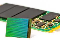
This new 3D NAND technology, jointly developed by Intel and Micron (via a joint venture called IM Flash), stacks layers of data storage cells vertically to create storage devices with three times higher capacity than existing flash memory formats such as SD cards and USB sticks.
This enables more storage in a smaller space, low power usage and high performance.
Micrton and Intel say this is the next step for memory technology, as the existing ‘planar’ flash memory is nearing its capacity limits.
‘So what’s this got to do with me?’ might be the question a camera retailer is asking if they have come this far in this story. With the latest enthusiast cameras equipped with 20+-heading-for-50-megapixel sensors, and capable of 4K video and up to 9 frames per second still capture at full resolution, capacity and upload/download speed of storage cards is critical. They are potentially a bottleneck for optimal performance of new and next-generation high-performance cameras. Photo retailers have an opportunity – and arguably a responsibility to their customers – to be memory technology experts. While we won’t be seeing a 3D NAND SD card in a camera this year, this is the leading edge of the technology. (And besides, it’s a slow news week!)
Micron and Intel say that ‘3D NAND technology is poised to make a dramatic impact by keeping flash storage solutions aligned with Moore’s Law, the trajectory for continued performance gains and cost savings, driving more widespread use of flash storage.’
‘This 3D NAND technology has the potential to create fundamental market shifts. The depth of the impact that flash has had to date—from smartphones to flash-optimised supercomputing—is really just scratching the surface of what’s possible,’ said Brian Shirley, vice president of Memory Technology and Solutions at Micron Technology.
The new 3D NAND technology stacks flash cells vertically in 32 layers to achieve 256GB multilevel cell (MLC) and 384Gb triple-level cell (TLC) die that fit within a standard package. These capacities can enable ‘gum stick-sized’ SSDs with more than 3.5TB of storage and standard 2.5-inch SSDs with greater than 10TB. Because capacity is achieved by stacking cells vertically, the individual cell dimensions can be considerably larger.
Key features:
Large capacities: Three-fourths of a terabyte will fit in a single fingertip-sized package;
Reduced cost per GB – First-generation 3D NAND is architected to achieve better cost efficiencies than planar NAND.
High read/write bandwidth, I/O speeds and random read performance.
Green: New sleep modes enable low-power use by cutting power to inactive NAND die (even when other die in the same package are active), dropping power consumption significantly in standby mode.
Improved latency and increased endurance.
Both 256GB and 384GB devices will be in full production by the fourth quarter of this year, according to Micron and Intel. Both companies are also developing individual lines of SSD solutions based on 3D NAND technology and expect those products to be available within the next year.


Be First to Comment